Difference between revisions of "Intel Xeon Phi and High Bandwidth Memory"
Pthomadakis (talk | contribs) (→Technology) |
Pthomadakis (talk | contribs) (→Resources) |
||
| (22 intermediate revisions by the same user not shown) | |||
| Line 1: | Line 1: | ||
| + | = High Bandwith Memory = | ||
High Bandwidth Memory (HBM) is a high bandwidth RAM interface for 3D-stacked DRAM developed by AMD. Hybrid Memory Cube Interface developed by Micron Technology is also a similar technology but is not compatible with HBM. HBM has been designed to provide higher bandwidth than DDR4 (for CPUs) and GDDR5 (for GPUs) while demanding less power and space. Furthermore, it is compatible with on-chip integration, while other technologies (DRAM, NAND) are not, which allows for even higher performance benefit. | High Bandwidth Memory (HBM) is a high bandwidth RAM interface for 3D-stacked DRAM developed by AMD. Hybrid Memory Cube Interface developed by Micron Technology is also a similar technology but is not compatible with HBM. HBM has been designed to provide higher bandwidth than DDR4 (for CPUs) and GDDR5 (for GPUs) while demanding less power and space. Furthermore, it is compatible with on-chip integration, while other technologies (DRAM, NAND) are not, which allows for even higher performance benefit. | ||
== Technology == | == Technology == | ||
| − | HBM consists of a number of stacked DRAM dies, with each one having a set of independent channels available to for access by the processors. | + | [[File:HBM 9 Comparison.png|520px|right|thumb|'''Comparison between DDR RAM and HBM''']] |
| − | [[File:HBM | + | [[File:hbm cpu.png|320px|right|thumb|'''HBM with CPU/GPU''']] |
| + | HBM consists of a number of stacked DRAM dies, with each one having a set of independent channels available to for access by the processors. Each channel interface maintains a 128-bit data bus operating at DDR data rates. The DRAM dies connect to the CPU or GPU through an ultra-fast interconnect called the “interposer. Several stacks of HBM are plugged into the interposer alongside a CPU or GPU, and that assembled module connects to a circuit board. Though these HBM stacks are not physically integrated with the CPU or GPU, they are so closely and quickly connected via the interposer that HBM’s characteristics are nearly indistinguishable from on-chip integrated RAM. | ||
| + | |||
| + | == Resources == | ||
| + | *[https://www.amd.com/en/technologies/hbm AMD High Bandwidth Memory] | ||
| + | *[https://ieeexplore.ieee.org/document/7939084/ HBM (High Bandwidth Memory) DRAM Technology and Architecture] | ||
| + | *[https://www.cs.utah.edu/thememoryforum/mike.pdf Nvidia on HBM] | ||
| + | |||
| + | |||
| + | |||
| + | |||
| + | |||
| + | |||
| + | |||
| + | |||
| + | |||
| + | |||
| + | |||
| + | |||
| + | |||
| + | |||
| + | = Intel Xeon Phi = | ||
| + | Xeon Phi is a series of x86 manycore processors designed and made entirely by Intel. They are intended for use in supercomputers, servers, and high-end workstations. Its architecture allows the use of standard programming languages and APIs such as OpenMP. Xeon Phis were originally designed based on a GPU architecture, being used as an external co-processor and requiring a host processor. The main difference with common GPUs like AMD's and Nvidia's counterparts is that they are x86 compatible requiring less effort to transit from a standard x86 processor to a Phi. | ||
| + | |||
| + | == Knights Landing == | ||
| + | The second Xeon Phi generation codenamed "Knights Landing" (KNL) is the first self-boot Phi processor that is compatible with x86 architecture. It can be used as a standalone processor running standard OS. Current versions number up to 72 cores with 4 threads per core, to a total of 288 threads per unit. | ||
| + | |||
| + | == Architecture == | ||
| + | The 72 cores running at ~ 1.3 GHz are split into tiles with 2 tiles per core, 2 VPUs ( Vector Processing Units, 512-bits) per core and each tile shares 2MB of L2 cache for a total of 36MB of L2 across the design. Tiles are arranged in a mesh topology using interconnected fabric. KNL incorporates Intel's version of high-bandwidth memory, named MCDRAM (Multi-Channel DRAM), promising about to 400+ GB/s bandwidth when all memory is used in parallel. Because of the cost of the memory and the need to keep it small and in-package, its size is limited to 16 GB. DDR4 RAM controllers are attached and DDR memory is a totally separate component of memory. | ||
| + | |||
| + | == MCDRAM == | ||
| + | MCDRAM is a high bandwidth (~4x more than DDR4), low capacity (up to 16GB) memory, packaged with the Knights Landing Silicon. MCDRAM can be configured as a third level cache (memory side cache) or as a distinct NUMA node (allocatable memory) or somewhere in between. With the different memory modes by which the system can be booted, it becomes very challenging from a software perspective to understand the best mode suitable for an application. At the same time, it is also very essential to utilize the available memory bandwidth in MCDRAM efficiently without leaving any performance on the table. Even thought MCDRAM offers a much higher bandwidth when used appropriately, its latencies are similar/higher to DDR access. | ||
| + | |||
| + | === HBM Modes === | ||
| + | [[File:HMB_Modes.png]] | ||
| + | |||
| + | HBM can work in three modes, which have to be determined by the BIOS and thus require a reboot in order to switch between them. The three modes are cache, flat and hybrid. | ||
| + | |||
| + | ==== Cache Mode ==== | ||
| + | In cache mode, the application needs no modification as the memory is used as cache controlled by the hardware. When the data are found in the cache there is a bandwidth memory as there is no movement out of the package, however, cache misses have an increased latency since they first need to check MCDRAM and then access DDR RAM compared to accessing directly the DDR RAM. | ||
| + | * Advantages | ||
| + | ** No software modifications required | ||
| + | ** Bandwidth benefit (over DDR) | ||
| + | * Disadvantages | ||
| + | ** Higher latency for DDR access. Needs to go through the MCDRAM first (i.e cache misses) | ||
| + | ** Misses limited by DDR bandwidth | ||
| + | |||
| + | ==== Flat Mode ==== | ||
| + | In flat mode, MCDRAM is mapped to the physical address space as a separate NUMA node that needs to be explicitly controlled by the application. | ||
| + | * Advantages | ||
| + | ** Application can have the maximum bandwidth | ||
| + | ** Lower latency ( no MCDRAM misses) | ||
| + | ** Maximum addressable memory | ||
| + | * Disadvantages | ||
| + | ** Code modification required | ||
| + | ** Application should decide what data to allocate where | ||
| + | ** Adds Complexity | ||
| + | |||
| + | ==== Hybrid Mode ==== | ||
| + | The memory is used in part as cache and the rest as a separate memory module. Has benefits and disadvantages of both. The portion that is assigned to its functionality is determined in boot time. | ||
| + | |||
| + | == Accessing MCDRAM in Flat Mode == | ||
| + | There are 2 options to control MCDRAM in flat mode with less or more control over individual allocations numactl and memkind library. | ||
| + | |||
| + | === Using numactl === | ||
| + | One can use numactl to configure the application to reserve memory from the MCDRAM without changing the code itself. Works better when the whole application can fit in the MCDRAM, but can still be used for bigger applications, by moving allocations that do not fit in MCDRAM to DDR. Another mode is to interleave allocation between the memory nodes. | ||
| + | |||
| + | === Using memkind library === | ||
| + | Memkind library is a user-extensible heap manager built on top of jemalloc, a C library for general-purpose memory allocation functions. The library is generalizable to any NUMA architecture, but for Knights Landing processors it is used primarily for manual allocation to HBM using special allocators for C/C++ | ||
| + | |||
| + | == KNL Mesh Interconnect == | ||
| + | [[File:knl_mesh.png|480px|right|thumb|'''KNL Mesh Interconnect''']] | ||
| + | KNL uses a mesh interconnect for the connection of the tiles containing the cores. The interconnect provides cache coherency using a distributed directory to filter snoops. It offers 3 clustering modes all-to-all, quadrant and sub-NUMA. | ||
| + | |||
| + | === All-to-All Mode === | ||
| + | The address is uniformly hashed across all distributed directories. There is no memory affinity between tile, directory, and memory. A miss in the L2 cache could cause memory accesses anywhere in the mesh. It is the most general and lowest performance mode, but it requires no modification to the source. | ||
| + | |||
| + | === Quadrant Mode === | ||
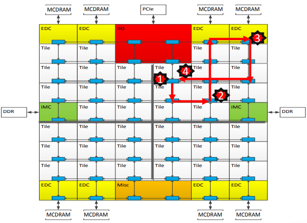
| + | Chip is divided into four virtual quadrants. The address is hashed to a directory in the same quadrant as the memory. This enables affinity between the directory and the memory, thus reducing how far the next memory access will happen. Lower latency and higher bandwidth than the All-to-All mode and still no changes are required to the source code. | ||
| + | |||
| + | === Sub-NUMA Clustering Mode === | ||
| + | In this mode, each quadrant is exposed as a separate NUMA domain to the operating system. Memory affinity can now be guaranteed between tile, directory, and memory. However, the application needs to be optimized for NUMA in order to get benefit. When optimized, it provides the lowest latency and highest bandwidth from all modes, by keeping the communication local to a single quadrant. | ||
| + | |||
| + | |||
| + | |||
| + | |||
| + | <gallery class="center" mode=packed widths="480px" heights="320px" caption="The diagrams below show the path followed in order to retrive data in case of a cache miss"> | ||
| + | File:mesh_all_to_all.png|'''(a) All-to-All Mode''' | ||
| + | File:mesh_quadrant.png|'''(b) Quadrant Mode''' | ||
| + | File:mesh_subnuma.png|'''(c) Sub-NUMA Mode''' | ||
| + | </gallery> | ||
| + | |||
| + | <div align="center">'''The numbers in the paths represent the following: (1) L2 cache miss (2) Directrory Access (3) Memory Access (4) Data return'''</div> | ||
| + | |||
| + | == Resources == | ||
| + | *[https://arxiv.org/pdf/1704.08273.pdf Exploring the Performance Benefit of Hybrid Memory System on HPC Environments (Paper)] | ||
| + | *[http://pages.cs.wisc.edu/~david/courses/cs758/Fall2016/handouts/restricted/Knights-landing.pdf KNL Paper] | ||
| + | *[https://software.intel.com/en-us/articles/mcdram-high-bandwidth-memory-on-knights-landing-analysis-methods-tools MCDRAM] | ||
Latest revision as of 16:34, 11 June 2018
Contents
High Bandwith Memory
High Bandwidth Memory (HBM) is a high bandwidth RAM interface for 3D-stacked DRAM developed by AMD. Hybrid Memory Cube Interface developed by Micron Technology is also a similar technology but is not compatible with HBM. HBM has been designed to provide higher bandwidth than DDR4 (for CPUs) and GDDR5 (for GPUs) while demanding less power and space. Furthermore, it is compatible with on-chip integration, while other technologies (DRAM, NAND) are not, which allows for even higher performance benefit.
Technology
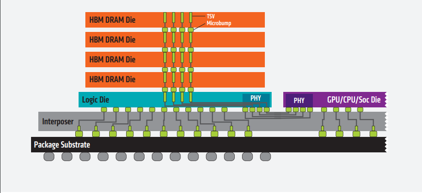
HBM consists of a number of stacked DRAM dies, with each one having a set of independent channels available to for access by the processors. Each channel interface maintains a 128-bit data bus operating at DDR data rates. The DRAM dies connect to the CPU or GPU through an ultra-fast interconnect called the “interposer. Several stacks of HBM are plugged into the interposer alongside a CPU or GPU, and that assembled module connects to a circuit board. Though these HBM stacks are not physically integrated with the CPU or GPU, they are so closely and quickly connected via the interposer that HBM’s characteristics are nearly indistinguishable from on-chip integrated RAM.
Resources
- AMD High Bandwidth Memory
- HBM (High Bandwidth Memory) DRAM Technology and Architecture
- Nvidia on HBM
Intel Xeon Phi
Xeon Phi is a series of x86 manycore processors designed and made entirely by Intel. They are intended for use in supercomputers, servers, and high-end workstations. Its architecture allows the use of standard programming languages and APIs such as OpenMP. Xeon Phis were originally designed based on a GPU architecture, being used as an external co-processor and requiring a host processor. The main difference with common GPUs like AMD's and Nvidia's counterparts is that they are x86 compatible requiring less effort to transit from a standard x86 processor to a Phi.
Knights Landing
The second Xeon Phi generation codenamed "Knights Landing" (KNL) is the first self-boot Phi processor that is compatible with x86 architecture. It can be used as a standalone processor running standard OS. Current versions number up to 72 cores with 4 threads per core, to a total of 288 threads per unit.
Architecture
The 72 cores running at ~ 1.3 GHz are split into tiles with 2 tiles per core, 2 VPUs ( Vector Processing Units, 512-bits) per core and each tile shares 2MB of L2 cache for a total of 36MB of L2 across the design. Tiles are arranged in a mesh topology using interconnected fabric. KNL incorporates Intel's version of high-bandwidth memory, named MCDRAM (Multi-Channel DRAM), promising about to 400+ GB/s bandwidth when all memory is used in parallel. Because of the cost of the memory and the need to keep it small and in-package, its size is limited to 16 GB. DDR4 RAM controllers are attached and DDR memory is a totally separate component of memory.
MCDRAM
MCDRAM is a high bandwidth (~4x more than DDR4), low capacity (up to 16GB) memory, packaged with the Knights Landing Silicon. MCDRAM can be configured as a third level cache (memory side cache) or as a distinct NUMA node (allocatable memory) or somewhere in between. With the different memory modes by which the system can be booted, it becomes very challenging from a software perspective to understand the best mode suitable for an application. At the same time, it is also very essential to utilize the available memory bandwidth in MCDRAM efficiently without leaving any performance on the table. Even thought MCDRAM offers a much higher bandwidth when used appropriately, its latencies are similar/higher to DDR access.
HBM Modes
HBM can work in three modes, which have to be determined by the BIOS and thus require a reboot in order to switch between them. The three modes are cache, flat and hybrid.
Cache Mode
In cache mode, the application needs no modification as the memory is used as cache controlled by the hardware. When the data are found in the cache there is a bandwidth memory as there is no movement out of the package, however, cache misses have an increased latency since they first need to check MCDRAM and then access DDR RAM compared to accessing directly the DDR RAM.
- Advantages
- No software modifications required
- Bandwidth benefit (over DDR)
- Disadvantages
- Higher latency for DDR access. Needs to go through the MCDRAM first (i.e cache misses)
- Misses limited by DDR bandwidth
Flat Mode
In flat mode, MCDRAM is mapped to the physical address space as a separate NUMA node that needs to be explicitly controlled by the application.
- Advantages
- Application can have the maximum bandwidth
- Lower latency ( no MCDRAM misses)
- Maximum addressable memory
- Disadvantages
- Code modification required
- Application should decide what data to allocate where
- Adds Complexity
Hybrid Mode
The memory is used in part as cache and the rest as a separate memory module. Has benefits and disadvantages of both. The portion that is assigned to its functionality is determined in boot time.
Accessing MCDRAM in Flat Mode
There are 2 options to control MCDRAM in flat mode with less or more control over individual allocations numactl and memkind library.
Using numactl
One can use numactl to configure the application to reserve memory from the MCDRAM without changing the code itself. Works better when the whole application can fit in the MCDRAM, but can still be used for bigger applications, by moving allocations that do not fit in MCDRAM to DDR. Another mode is to interleave allocation between the memory nodes.
Using memkind library
Memkind library is a user-extensible heap manager built on top of jemalloc, a C library for general-purpose memory allocation functions. The library is generalizable to any NUMA architecture, but for Knights Landing processors it is used primarily for manual allocation to HBM using special allocators for C/C++
KNL Mesh Interconnect
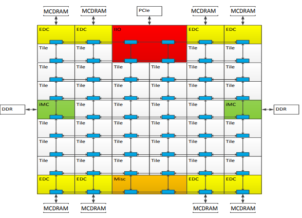
KNL uses a mesh interconnect for the connection of the tiles containing the cores. The interconnect provides cache coherency using a distributed directory to filter snoops. It offers 3 clustering modes all-to-all, quadrant and sub-NUMA.
All-to-All Mode
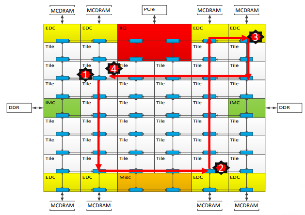
The address is uniformly hashed across all distributed directories. There is no memory affinity between tile, directory, and memory. A miss in the L2 cache could cause memory accesses anywhere in the mesh. It is the most general and lowest performance mode, but it requires no modification to the source.
Quadrant Mode
Chip is divided into four virtual quadrants. The address is hashed to a directory in the same quadrant as the memory. This enables affinity between the directory and the memory, thus reducing how far the next memory access will happen. Lower latency and higher bandwidth than the All-to-All mode and still no changes are required to the source code.
Sub-NUMA Clustering Mode
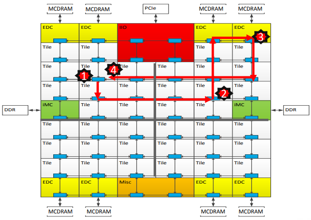
In this mode, each quadrant is exposed as a separate NUMA domain to the operating system. Memory affinity can now be guaranteed between tile, directory, and memory. However, the application needs to be optimized for NUMA in order to get benefit. When optimized, it provides the lowest latency and highest bandwidth from all modes, by keeping the communication local to a single quadrant.
- The diagrams below show the path followed in order to retrive data in case of a cache miss

